Russia, Moscow


СДЕЛАЙТЕ СВОИ УРОКИ ЕЩЁ ЭФФЕКТИВНЕЕ, А ЖИЗНЬ СВОБОДНЕЕ
Благодаря готовым учебным материалам для работы в классе и дистанционно
Скидки до 50 % на комплекты
только до
Готовые ключевые этапы урока всегда будут у вас под рукой
Организационный момент
Проверка знаний
Объяснение материала
Закрепление изученного
Итоги урока

Была в сети 17.05.2024 18:53

Ivanova Elvira Vitalievna
English teacher
3 года
Местоположение
Специализация
Elektronenstrahllithografiesysteme
Категория:
Информатика
07.04.2022 14:24

Просмотр содержимого документа
«Elektronenstrahllithografiesysteme»
Lecture 2 Electron Beam Lithography
Author of presentation
Ivanova Elvira
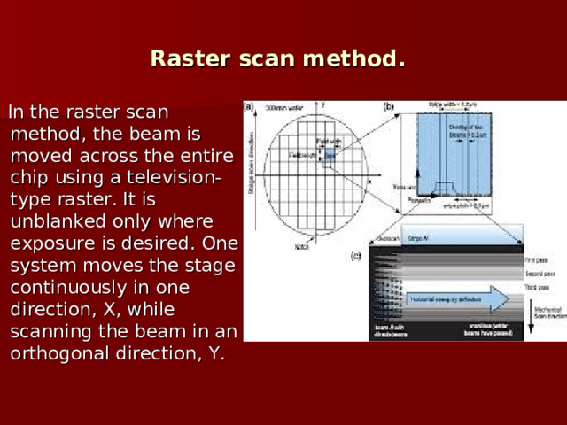
Raster scan method.
In the raster scan method, the beam is moved across the entire chip using a television-type raster. It is unblanked only where exposure is desired. One system moves the stage continuously in one direction, X, while scanning the beam in an orthogonal direction, Y.
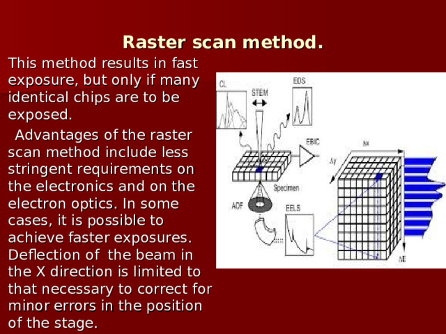
Raster scan method.
- This method results in fast exposure, but only if many identical chips are to be exposed.
Advantages of the raster scan method include less stringent requirements on the electronics and on the electron optics. In some cases, it is possible to achieve faster exposures. Deflection of the beam in the X direction is limited to that necessary to correct for minor errors in the position of the stage.
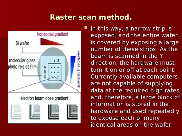
Raster scan method.
- In this way, a narrow strip is exposed, and the entire wafer is covered by exposing a large number of these strips. As the beam is scanned in the Y direction, the hardware must turn it on or off at each point. Currently available computers are not capable of supplying data at the required high rates and, therefore, a large block of information is stored in the hardware and used repeatedly to expose each of many identical areas on the wafer.
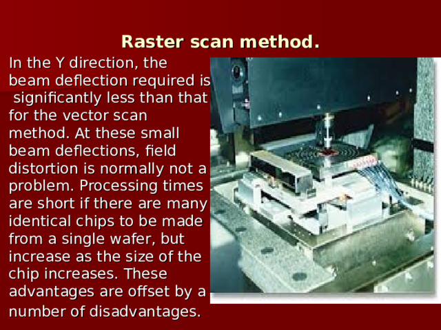
Raster scan method.
- In the Y direction, the beam deflection required is significantly less than that for the vector scan method. At these small beam deflections, field distortion is normally not a problem. Processing times are short if there are many identical chips to be made from a single wafer, but increase as the size of the chip increases. These advantages are offset by a number of disadvantages.
Raster scan method.
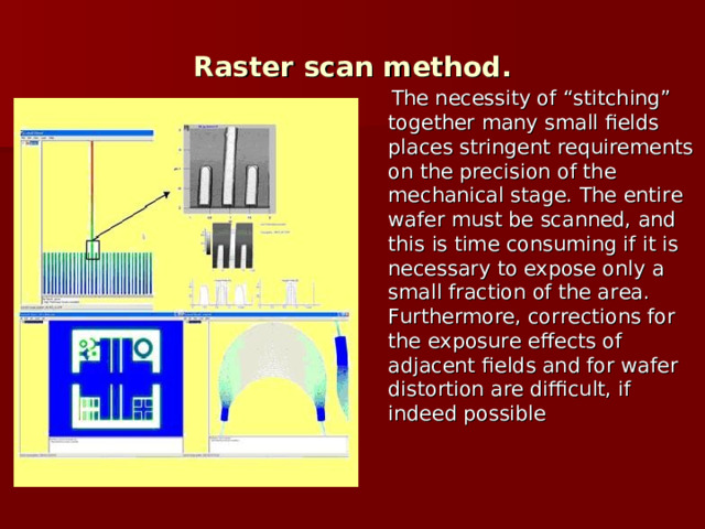
The necessity of “stitching” together many small fields places stringent requirements on the precision of the mechanical stage. The entire wafer must be scanned, and this is time consuming if it is necessary to expose only a small fraction of the area. Furthermore, corrections for the exposure effects of adjacent fields and for wafer distortion are difficult, if indeed possible
Vector scan method.
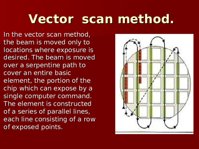
- In the vector scan method, the beam is moved only to locations where exposure is desired. The beam is moved over a serpentine path to cover an entire basic element, the portion of the chip which can expose by a single computer command. The element is constructed of a series of parallel lines, each line consisting of a row of exposed points.
Vector scan method.
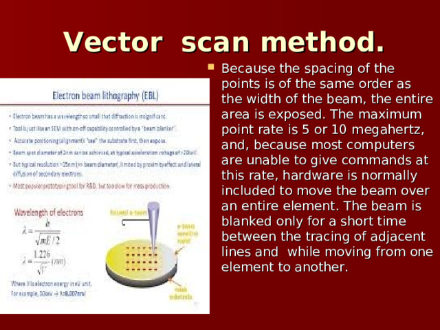
- Because the spacing of the points is of the same order as the width of the beam, the entire area is exposed. The maximum point rate is 5 or 10 megahertz, and, because most computers are unable to give commands at this rate, hardware is normally included to move the beam over an entire element. The beam is blanked only for a short time between the tracing of adjacent lines and while moving from one element to another.
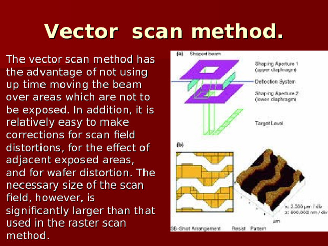
Vector scan method.
- The vector scan method has the advantage of not using up time moving the beam over areas which are not to be exposed. In addition, it is relatively easy to make corrections for scan field distortions, for the effect of adjacent exposed areas, and for wafer distortion. The necessary size of the scan field, however, is significantly larger than that used in the raster scan method.
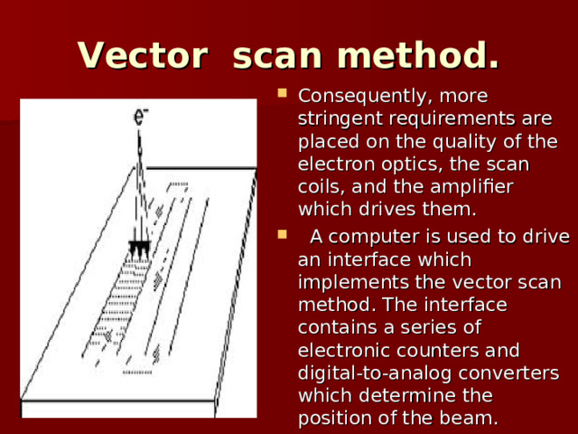
Vector scan method.
- Consequently, more stringent requirements are placed on the quality of the electron optics, the scan coils, and the amplifier which drives them.
- A computer is used to drive an interface which implements the vector scan method. The interface contains a series of electronic counters and digital-to-analog converters which determine the position of the beam.
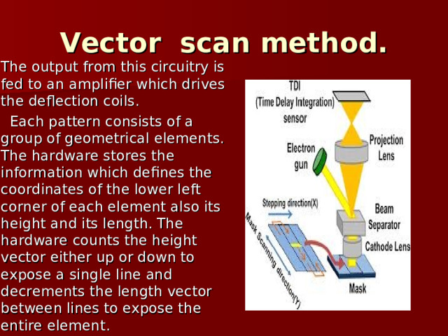
Vector scan method.
- The output from this circuitry is fed to an amplifier which drives the deflection coils.
- Each pattern consists of a group of geometrical elements. The hardware stores the information which defines the coordinates of the lower left corner of each element also its height and its length. The hardware counts the height vector either up or down to expose a single line and decrements the length vector between lines to expose the entire element.
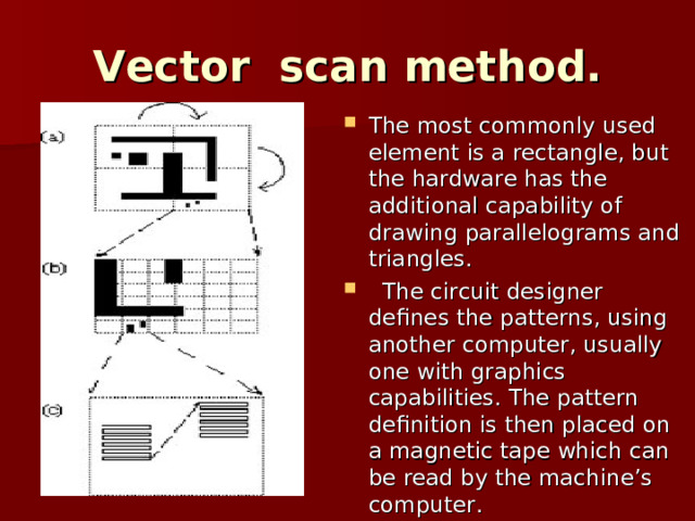
Vector scan method.
- The most commonly used element is a rectangle, but the hardware has the additional capability of drawing parallelograms and triangles.
- The circuit designer defines the patterns, using another computer, usually one with graphics capabilities. The pattern definition is then placed on a magnetic tape which can be read by the machine’s computer.
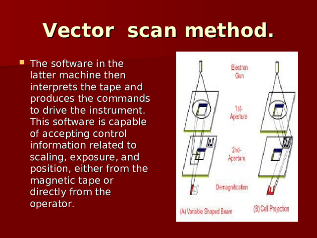
Vector scan method.
- The software in the latter machine then interprets the tape and produces the commands to drive the instrument. This software is capable of accepting control information related to scaling, exposure, and position, either from the magnetic tape or directly from the operator.
Difference between Raster Scan System and Random Scan System
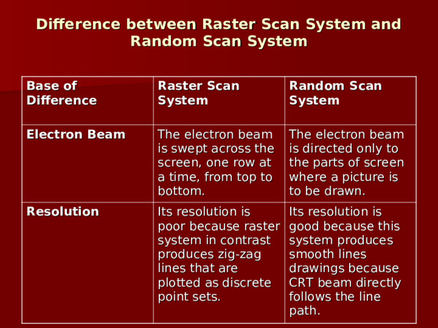
Base of Difference
Raster Scan System
Electron Beam
Random Scan System
The electron beam is swept across the screen, one row at a time, from top to bottom.
Resolution
Its resolution is poor because raster system in contrast produces zig-zag lines that are plotted as discrete point sets.
The electron beam is directed only to the parts of screen where a picture is to be drawn.
Its resolution is good because this system produces smooth lines drawings because CRT beam directly follows the line path.
Difference between Raster Scan System and Random Scan System
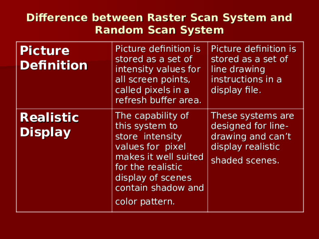
Picture Definition
Picture definition is stored as a set of intensity values for all screen points, called pixels in a refresh buffer area.
Realistic Display
Picture definition is stored as a set of line drawing instructions in a display file.
The capability of this system to store intensity values for pixel makes it well suited for the realistic display of scenes contain shadow and color pattern.
These systems are designed for line-drawing and can’t display realistic shaded scenes.
Difference between Raster Scan System and Random Scan System
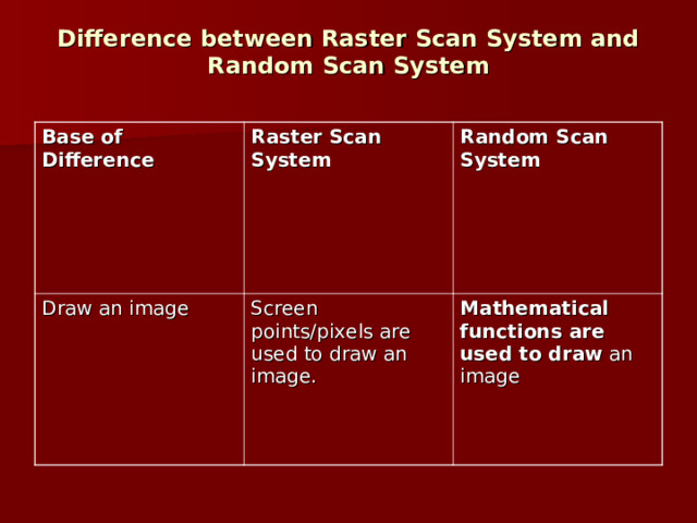
Base of Difference
Raster Scan System
Draw an image
Random Scan System
Screen points/pixels are used to draw an image.
Mathematical functions are used to draw an image


Вебинар для учителей

Свидетельство об участии БЕСПЛАТНО!
Полезное для учителя

Реализация образовательных программ осуществляется с применением исключительно электронного обучения и ДОТ