Russia, Moscow


СДЕЛАЙТЕ СВОИ УРОКИ ЕЩЁ ЭФФЕКТИВНЕЕ, А ЖИЗНЬ СВОБОДНЕЕ
Благодаря готовым учебным материалам для работы в классе и дистанционно
Скидки до 50 % на комплекты
только до
Готовые ключевые этапы урока всегда будут у вас под рукой
Организационный момент
Проверка знаний
Объяснение материала
Закрепление изученного
Итоги урока

Была в сети 17.05.2024 18:53

Ivanova Elvira Vitalievna
English teacher
3 года
Местоположение
Специализация
Lecture8 FINE PATTERN GENERATION WITH SHAPED-BEAM DIRECT WRITING LITHOGRAPHY
Категория:
Информатика
09.04.2022 14:49

Просмотр содержимого документа
«Lecture8 FINE PATTERN GENERATION WITH SHAPED-BEAM DIRECT WRITING LITHOGRAPHY»
FINE PATTERN GENERATION WITH SHAPED-BEAM DIRECT WRITING LITHOGRAPHY
Author of presentation
Ivanova Elvira
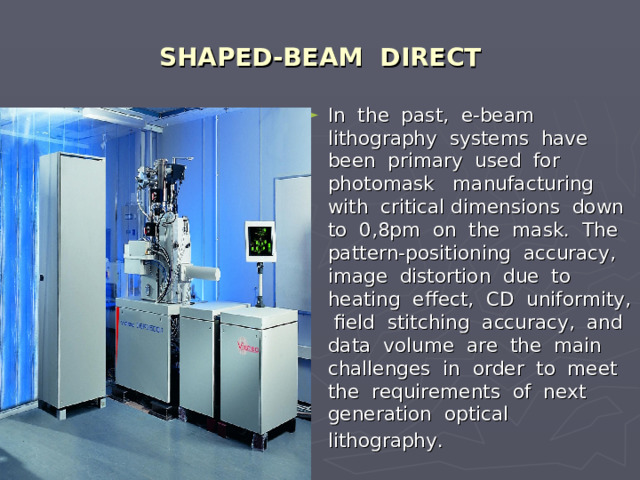
SHAPED-BEAM DIRECT
- In the past, e-beam lithography systems have been primary used for photomask manufacturing with critical dimensions down to 0,8pm on the mask. The pattern-positioning accuracy, image distortion due to heating effect, CD uniformity, field stitching accuracy, and data volume are the main challenges in order to meet the requirements of next generation optical lithography.
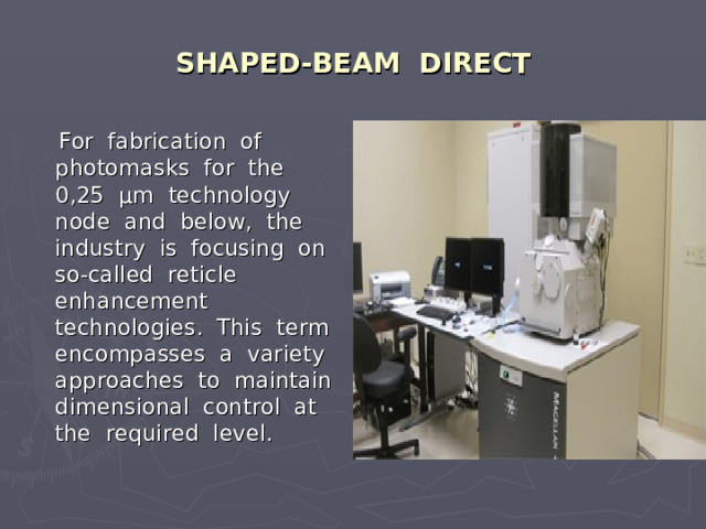
SHAPED-BEAM DIRECT
For fabrication of photomasks for the 0,25 μm technology node and below, the industry is focusing on so-called reticle enhancement technologies. This term encompasses a variety approaches to maintain dimensional control at the required level.
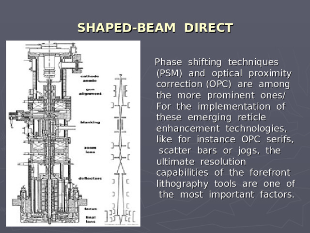
SHAPED-BEAM DIRECT
Phase shifting techniques (PSM) and optical proximity correction (OPC) are among the more prominent ones/ For the implementation of these emerging reticle enhancement technologies, like for instance OPC serifs, scatter bars or jogs, the ultimate resolution capabilities of the forefront lithography tools are one of the most important factors.
SHAPED-BEAM DIRECT
For these specific patterns the consensus is at least half of the nx- feature size of the relevant device generation. In consequence, for the 0,25 μm technology node , the mask lithographers have to have the potential to generate features of 400nm on the critical level 4x-masks, the 0,18 μm needs demands 280 nm and the 0,13 μm node which is assumed to become significant industrial relevance in 2002, demands 200nm.
Consequently to the stringent requirements of advanced mask-making technologies, the e-beam lithography of today has been developed to excellent patterning performance,
SHAPED-BEAM DIRECT
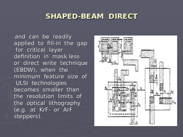
and can be readily applied to fill-in the gap for critical layer definition in mask less or direct write technique (EBDW), when the minimum feature size of ULSI technologies becomes smaller than the resolution limits of the optical lithography (e.g. at KrF- or ArF steppers).
SHAPED-BEAM DIRECT
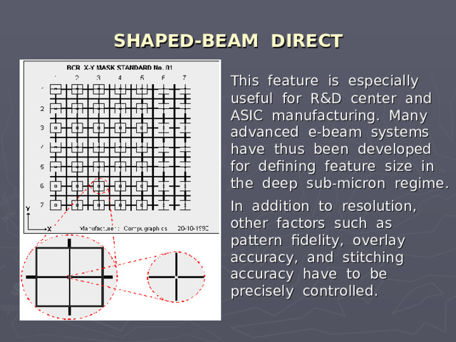
This feature is especially useful for R&D center and ASIC manufacturing. Many advanced e-beam systems have thus been developed for defining feature size in the deep sub-micron regime.
In addition to resolution, other factors such as pattern fidelity, overlay accuracy, and stitching accuracy have to be precisely controlled.
SHAPED-BEAM DIRECT
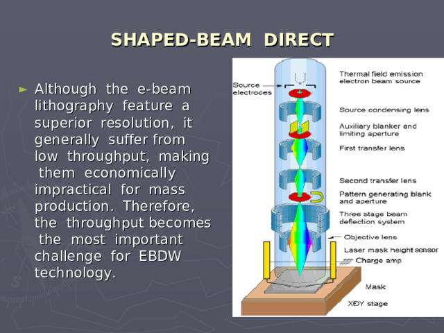
- Although the e-beam lithography feature a superior resolution, it generally suffer from low throughput, making them economically impractical for mass production. Therefore, the throughput becomes the most important challenge for EBDW technology.
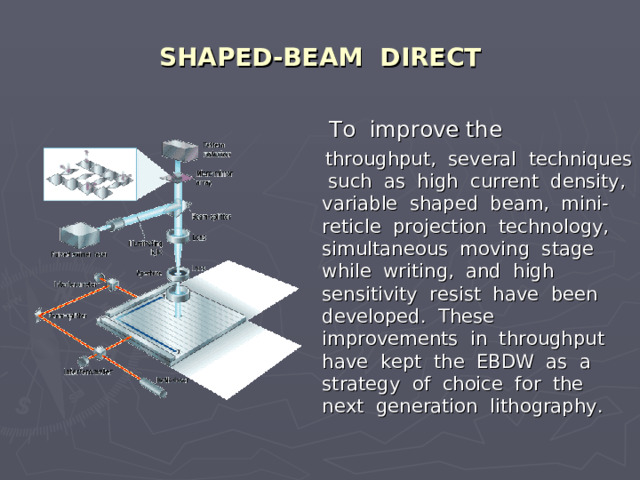
SHAPED-BEAM DIRECT
To improve the
throughput, several techniques such as high current density, variable shaped beam, mini-reticle projection technology, simultaneous moving stage while writing, and high sensitivity resist have been developed. These improvements in throughput have kept the EBDW as a strategy of choice for the next generation lithography.
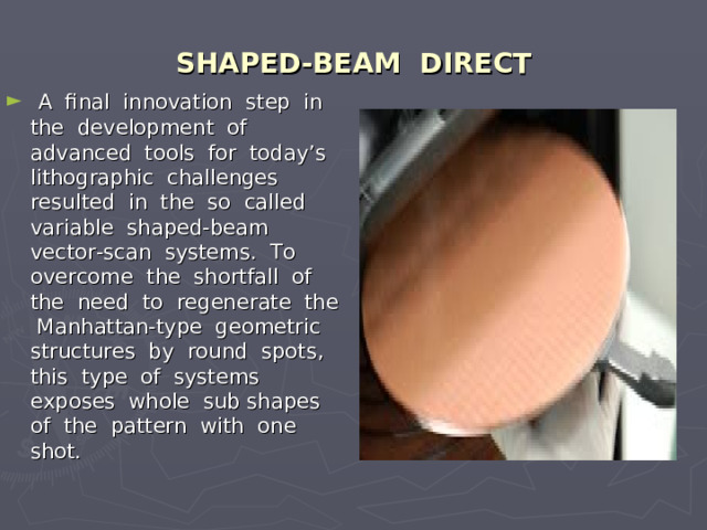
SHAPED-BEAM DIRECT
- A final innovation step in the development of advanced tools for today’s lithographic challenges resulted in the so called variable shaped-beam vector-scan systems. To overcome the shortfall of the need to regenerate the Manhattan-type geometric structures by round spots, this type of systems exposes whole sub shapes of the pattern with one shot.
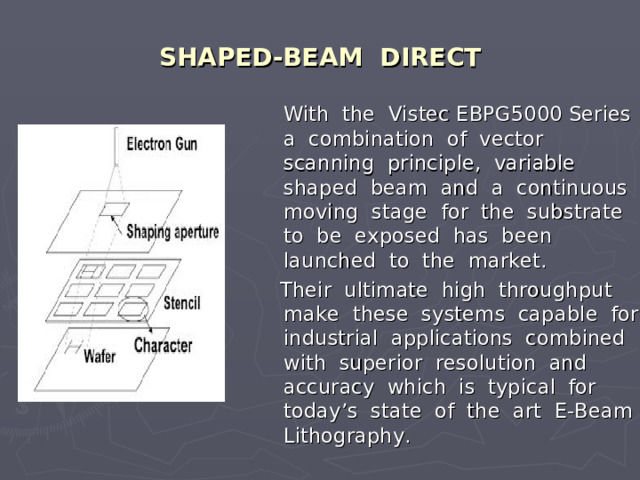
SHAPED-BEAM DIRECT
With the Vistec EBPG5000 Series a combination of vector scanning principle, variable shaped beam and a continuous moving stage for the substrate to be exposed has been launched to the market.
Their ultimate high throughput make these systems capable for industrial applications combined with superior resolution and accuracy which is typical for today’s state of the art E-Beam Lithography.


Вебинар для учителей

Свидетельство об участии БЕСПЛАТНО!
Полезное для учителя

Реализация образовательных программ осуществляется с применением исключительно электронного обучения и ДОТ