Russia, Moscow


СДЕЛАЙТЕ СВОИ УРОКИ ЕЩЁ ЭФФЕКТИВНЕЕ, А ЖИЗНЬ СВОБОДНЕЕ
Благодаря готовым учебным материалам для работы в классе и дистанционно
Скидки до 50 % на комплекты
только до
Готовые ключевые этапы урока всегда будут у вас под рукой
Организационный момент
Проверка знаний
Объяснение материала
Закрепление изученного
Итоги урока

Была в сети 17.05.2024 18:53

Ivanova Elvira Vitalievna
English teacher
3 года
Местоположение
Специализация
Elektronenstrahllithografie
Категория:
Информатика
07.04.2022 14:19

Просмотр содержимого документа
«Elektronenstrahllithografie»
Lecture 1 Electron Beam Lithography.
Author of presentation
Ivanova Elvira
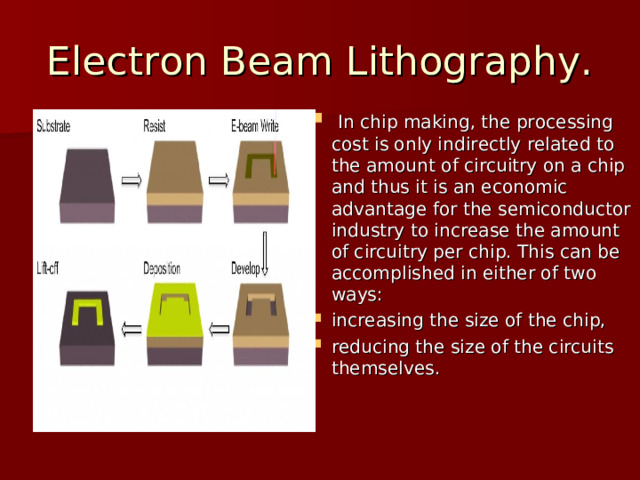
Electron Beam Lithography.
- In chip making, the processing cost is only indirectly related to the amount of circuitry on a chip and thus it is an economic advantage for the semiconductor industry to increase the amount of circuitry per chip. This can be accomplished in either of two ways:
- increasing the size of the chip,
- reducing the size of the circuits themselves.
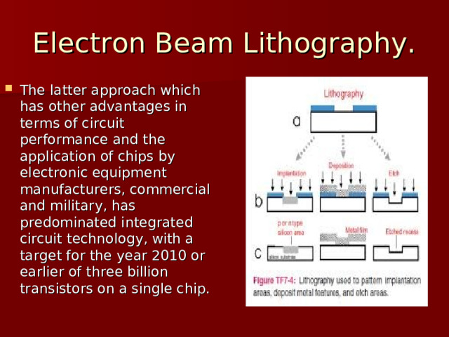
Electron Beam Lithography.
- The latter approach which has other advantages in terms of circuit performance and the application of chips by electronic equipment manufacturers, commercial and military, has predominated integrated circuit technology, with a target for the year 2010 or earlier of three billion transistors on a single chip.
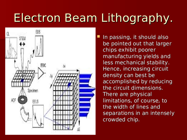
Electron Beam Lithography.
- In passing, it should also be pointed out that larger chips exhibit poorer manufacturing yields and less mechanical stability. Hence, increasing circuit density can best be accomplished by reducing the circuit dimensions. There are physical limitations, of course, to the width of lines and separations in an intensely crowded chip.
Electron Beam Lithography.
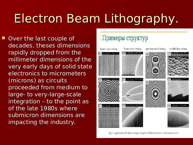
- Over the last couple of decades, theses dimensions rapidly dropped from the millimeter dimensions of the very early days of solid state electronics to micrometers (microns) as circuits proceeded from medium to large- to very-large-scale integration – to the point as of the late 1980s where submicron dimensions are impacting the industry.
Electron Beam Lithography.
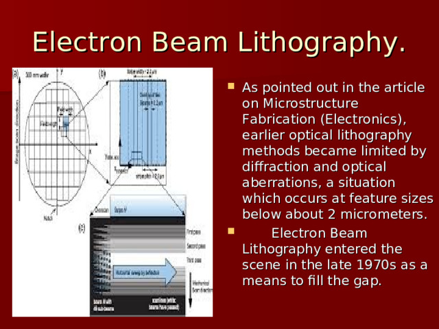
- As pointed out in the article on Microstructure Fabrication (Electronics), earlier optical lithography methods became limited by diffraction and optical aberrations, a situation which occurs at feature sizes below about 2 micrometers.
- Electron Beam Lithography entered the scene in the late 1970s as a means to fill the gap.
Principles of Electron Beam Lithography.
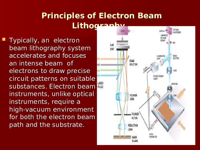
- Typically, an electron beam lithography system accelerates and focuses an intense beam of electrons to draw precise circuit patterns on suitable substances. Electron beam instruments, unlike optical instruments, require a high-vacuum environment for both the electron beam path and the substrate.
Principles of Electron Beam Lithography
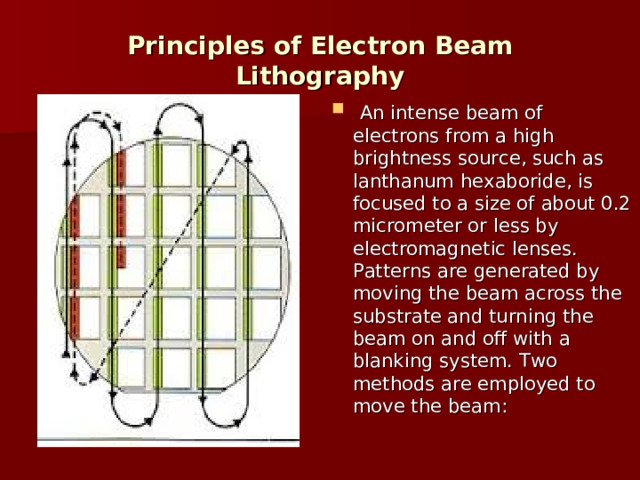
- An intense beam of electrons from a high brightness source, such as lanthanum hexaboride, is focused to a size of about 0.2 micrometer or less by electromagnetic lenses. Patterns are generated by moving the beam across the substrate and turning the beam on and off with a blanking system. Two methods are employed to move the beam:
Principles of Electron Beam Lithography
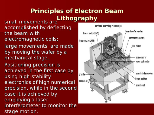
- small movements are accomplished by deflecting the beam with electromagnetic coils;
- large movements are made by moving the wafer by a mechanical stage.
- Positioning precision is achieved in the first case by using high-stability electronics of high numerical precision, while in the second case it is achieved by employing a laser interferometer to monitor the stage motion.
Principles of Electron Beam Lithography
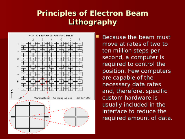
- Because the beam must move at rates of two to ten million steps per second, a computer is required to control the position. Few computers are capable of the necessary data rates and, therefore, specific custom hardware is usually included in the interface to reduce the required amount of data.
Principles of Electron Beam Lithography
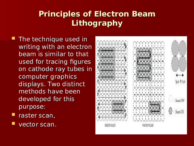
- The technique used in writing with an electron beam is similar to that used for tracing figures on cathode ray tubes in computer graphics displays. Two distinct methods have been developed for this purpose:
- raster scan,
- vector scan.
Principles of Electron Beam Lithography
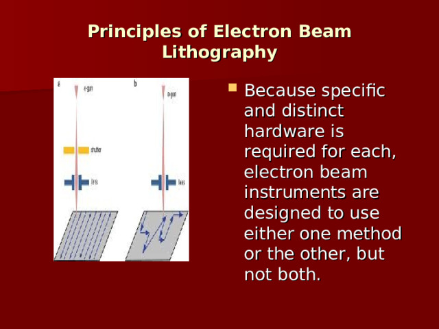
- Because specific and distinct hardware is required for each, electron beam instruments are designed to use either one method or the other, but not both.


Вебинар для учителей

Свидетельство об участии БЕСПЛАТНО!
Полезное для учителя

Реализация образовательных программ осуществляется с применением исключительно электронного обучения и ДОТ