Russia, Moscow

СДЕЛАЙТЕ СВОИ УРОКИ ЕЩЁ ЭФФЕКТИВНЕЕ, А ЖИЗНЬ СВОБОДНЕЕ
Благодаря готовым учебным материалам для работы в классе и дистанционно
Скидки до 50 % на комплекты
только до
Готовые ключевые этапы урока всегда будут у вас под рукой
Организационный момент
Проверка знаний
Объяснение материала
Закрепление изученного
Итоги урока
Была в сети 17.05.2024 18:53

Ivanova Elvira Vitalievna
English teacher
3 года
Местоположение
Специализация
Display device basic microfabrication techniques
Категория:
Информатика
08.04.2022 17:26

Просмотр содержимого документа
«Display device basic microfabrication techniques»
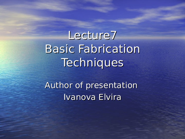
Lecture7 Basic Fabrication Techniques
Author of presentation
Ivanova Elvira
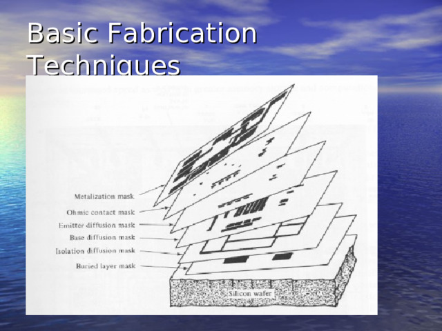
Basic Fabrication Techniques
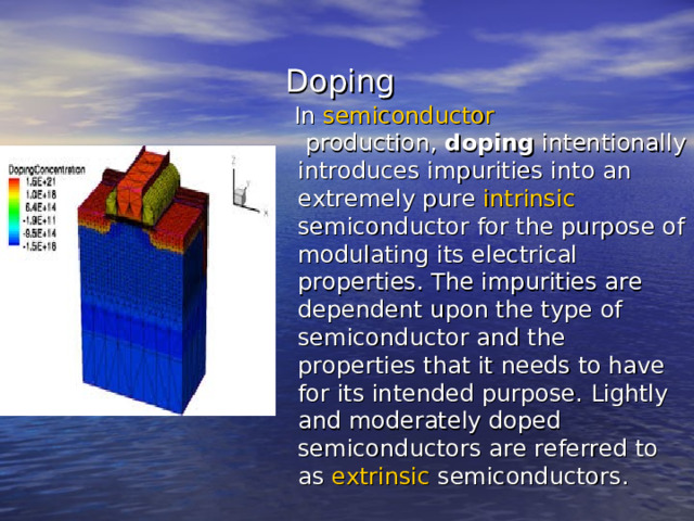
Doping
In semiconductor production, doping intentionally introduces impurities into an extremely pure intrinsic semiconductor for the purpose of modulating its electrical properties. The impurities are dependent upon the type of semiconductor and the properties that it needs to have for its intended purpose. Lightly and moderately doped semiconductors are referred to as extrinsic semiconductors .
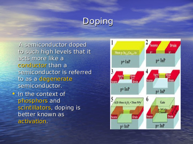
Doping
A semiconductor doped to such high levels that it acts more like a conductor than a semiconductor is referred to as a degenerate semiconductor .
- In the context of phosphors and scintillators , doping is better known as activation .
Doping
- The techniques used to make all the semiconductor devices have many features in common, whether these be diodes, transistors, four-layer controlled rectifiers, or other devices. For this reason, the processes employed to fabricate transistors are of general application.
- To achieve as large a current gain as possible within a transistor, the lifetime of the majority-charge carrier, in the base region, must be relatively long before recombination of a hole-electron pair takes place. This requires that the transistor be made from a single crystal of high quality. At the same time, to obtain other desirable transistor properties, the impurity content of the crystal must be accurately controlled. This is best achieved by refining the semiconductor material to maximum possible purity, and then adding impurities under carefully specified conditions through one of the available doping techniques.
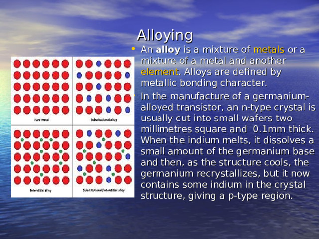
Alloying
- An alloy is a mixture of metals or a mixture of a metal and another element . Alloys are defined by metallic bonding character.
- In the manufacture of a germanium-alloyed transistor, an n-type crystal is usually cut into small wafers two millimetres square and 0.1mm thick. When the indium melts, it dissolves a small amount of the germanium base and then, as the structure cools, the germanium recrystallizes, but it now contains some indium in the crystal structure, giving a p-type region.
Alloying
- The alloying process is repeated on the other side of the base crystal to obtain the required two-junction structure. Contacts are soldered to the n-type base region and to the collector and emitter pellets. To minimize the base resistance the base contact is often in the form of a ring around the emitter. Since most of the power is developed at the collector, this part of the transistor is made physically larger than the emitter.
- It is difficult to alloy into a wafer of a thickness of less than 0.05mm and extremely difficult to make alloyed-junction transistors with a base width narrower than 0.025mm consistently. Also, the alloying process produces only a poorly defined boundary for the p-n junction. This results in a usable upper frequency limit of about ten megahertz for germanium-alloyed transistors. This technique has been superseded for the most part by other doping methods.
Diffusion
- Diffusion is the net movement of molecules or atoms from a region of high concentration to a region of low concentration. This is also referred to as the movement of a substance down a concentration gradient . A gradient is the change in the value of a quantity (e.g., concentration, pressure , temperature ) with the change in another variable (usually distance ). For example, a change in concentration over a distance is called a concentration gradient, a change in pressure over a distance is called a pressure gradient , and a change in temperature over a distance is a called a temperature gradient .
Ion implantation
- Ion implantation is a materials engineering process by which ions of a material are accelerated in an electrical field and impacted into a solid. This process is used to change the physical, chemical, or electrical properties of the solid. Ion implantation is used in semiconductor device fabrication and in metal finishing, as well as various applications in materials science research. The ions alter the elemental composition of the target (if the ions differ in composition from the target), stopping in the target and staying there.
Ion implantation
- They also cause many chemical and physical changes in the target by transferring their energy and momentum to the electrons and atomic nuclei of the target material. This causes a structural change, in that the crystal structure of the target can be damaged or even destroyed by the energetic collision cascades . Because the ions have masses comparable to those of the target atoms, they knock the target atoms out of place more than electron beams do. If the ion energy is sufficiently high (usually tens of MeV) to overcome the coulomb barrier , there can even be a small amount of nuclear transmutation.
Etching
- Etching is used in microfabrication to chemically remove layers from the surface of a wafer during manufacturing. Etching is a critically important process module, and every wafer undergoes many etching steps before it is complete.
- For many etch steps, part of the wafer is protected from the etchant by a "masking" material which resists etching. In some cases, the masking material is a photoresist which has been patterned usingphotolithography. Other situations require a more durable mask, such as silicon nitride.


Вебинар для учителей
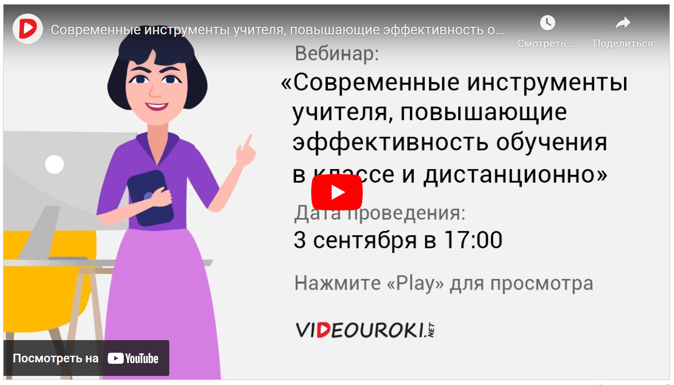
Свидетельство об участии БЕСПЛАТНО!
Полезное для учителя

Реализация образовательных программ осуществляется с применением исключительно электронного обучения и ДОТ